
advantages and disadvantages of scanning tunneling microscope
STMs are helpful because they can give researchers a three dimensional profile of a surface, which allows researchers to examine a multitude of characteristics, including roughness, surface defects and determining things about the molecules such as size and conformation. It provides a three-dimensional profile of the surface which is very useful for characterizing surface roughness, observing surface defects, and determining the size and conformation of MicroscopeMaster.com is a participant in the Amazon Services LLC Associates Program, an affiliate advertising program designed to provide a means to earn fees by linking to Amazon.com and affiliated sites. experiment. The barrier height is defined as the threshold at which electrons will cross the interface and are measurable as a current in the far collector. Additionally, micro-manipulation of molecules, DNA, biological and organic specimens using these precision instruments will produce a greater understanding of and new methods for: if(typeof ez_ad_units!='undefined'){ez_ad_units.push([[250,250],'microscopemaster_com-leader-1','ezslot_8',124,'0','0'])};__ez_fad_position('div-gpt-ad-microscopemaster_com-leader-1-0'); Scanning probe microscopes have improved microscopy research in many ways like the invention of the microscope improved the world. If the voltage is greater than the barrier height, useful information can be gathered about the magnitude of the current at the collector as opposed to the initial voltage. Usually (<> e|V|/2) is about 5 eV, which k0 about 1 -1, then I/I = 1/8. A wide variety of magnetic materials have been studied as possible coatings, including both ferromagnetic materials, such as a thin coat of iron or of gadolinium, and antiferromagnetic materials such as chromium. The diameter of the probe will influence STEMs spatial resolution, which is caused by the lens aberrations. At a metal/n-type semiconductor interface this is the difference between the conduction band minimum and the Fermi level. This renders not only enhanced images but specimen properties, response and reaction or non-action when specimens are stimulated or touched. The magnitude of this tunneling current is dependent on the bias voltage applied and the distance between the tip and the surface. Portable optical light microscopes are widely used tools in the field of microscopy. Check out this systems meld of the most powerful and versatile devices available., Return from Scanning Probe Microscope to Best Microscope Home. The electron cloud associated with metal atoms at a surface extends a very small distance above the surface. This information indicates that actually the functionalization levels of thiol- and thiophene-SWNTs are comparable. From AFM image, Au-thiol-SWNT (Figure \(\PageIndex{6}\)a) shows that most of the sidewalls are unfunctionalized, while Au-thiophene-SWNT (Figure \(\PageIndex{6}\) c)shows long bands of continuous functionalized regions on SWNT. In a typical case, with the atoms spaced five angstroms apart, there is a finite probability that the electron will penetrate the barrier and move to the adjacent atom. ) or https:// means youve safely connected to the .gov website. The force-distance dependence in AFM is much more complex when characteristics such as tip shape and contact force are considered. https://www.nist.gov/pml/scanning-tunneling-microscope/scanning-tunneling-microscope-introduction. Low cost and relatively low quality STMs start at approximately $8,000 but some people have actually built their own amateur STMs for much less than that amount. As discussed above, EELS detects the energy loss of electrons when they interact with samples and the specimen, then the thickness of samples will impact on the energy lost detection. The LibreTexts libraries arePowered by NICE CXone Expertand are supported by the Department of Education Open Textbook Pilot Project, the UC Davis Office of the Provost, the UC Davis Library, the California State University Affordable Learning Solutions Program, and Merlot. The tunneling current image should show a uniform background, but this is not the case. 4.3 Scanning Probe Microscopy. For example, the operation of TEM on samples sometimes result in blurring image and low contrast because of chromatic aberration. In this situation, the feedback control system will respond quickly and retract the tip. Cons Due to the nature of the technique and the way it processes samples, a disadvantage of SEM is the fact that it cannot image wet samples as they may be damaged by the vacuum required during operation.  Photon scanning tunneling microscopy (PSTM) measures light to determine more information about characteristic sample topography. STMs are based on the idea of quantum tunneling, when a conducting tip is brought very close to the surface and a voltage difference between the tip and the surface is applied. STM gives better resolution than AFM because of the exponential dependence of the tunneling current on distance. if(typeof ez_ad_units!='undefined'){ez_ad_units.push([[728,90],'microscopemaster_com-medrectangle-3','ezslot_4',148,'0','0'])};__ez_fad_position('div-gpt-ad-microscopemaster_com-medrectangle-3-0'); For an STM, good resolution is 0.1 nm lateral resolution and 0.01 nm depth resolution. WebThe scanning tunneling microscope (STM) works by scanning a very sharp metal wire tip over a surface. STMs are also versatile. for diagnosis or treatment. At close distances, the electron clouds of the metal tip overlap with the electron clouds of the surface atoms (Figure \(\PageIndex{9}\) inset). The probability of finding such tunneling electrons decreases exponentially as the distance from the surface increases. If it is necessary to measure small collector currents, such as with an interface of high-barrier-height, a high-gain, low-noise current preamplifier can be added to the system. PSTM shows much promise in the imaging of biological materials due to the increase in vertical resolution and the ability to measure a sample within a liquid environment with a high index TIR substrate and probe tip. EELS result shows the core-loss edge of La, Mn and O (Figure \(\PageIndex{25}\) c), but the researchers did not give information on core-loss edge of Sr, Sr has N2,3 edge at 29 eV and L3 edge at 1930 eV and L2 edge at 2010 eV. A current amplifier can covert the generated tunneling current into a voltage. MicroscopeMaster website is for educational purposes only. 4.3 Scanning Probe Microscopy. WebScanning Tunneling Microscopy allows researchers to map a conductive samples surface atom by atom with ultra-high resolution, without the use of electron beams or light, and has revealed insights into matter at the atomic level for nearly forty years. Other sample types, such as semiconductor interfaces or biological samples, need some enhancements to the traditional STM apparatus to yield more detailed sample information. MicroscopeMaster is not liable for your results or any They can be used in ultra high vacuum, air, water and other liquids and gasses. The scanning tunneling microscope (STM) is widely used in both industrial and fundamental research to obtain atomic-scale images of metal surfaces. Other advantages of the scanning tunneling microscope include: There are very few disadvantages to using a scanning tunneling microscope.if(typeof ez_ad_units!='undefined'){ez_ad_units.push([[580,400],'microscopemaster_com-banner-1','ezslot_11',111,'0','0'])};__ez_fad_position('div-gpt-ad-microscopemaster_com-banner-1-0'); The two major downsides to using STMs are: The electronics required for an STM are extremely sophisticated as well as very expensive.
 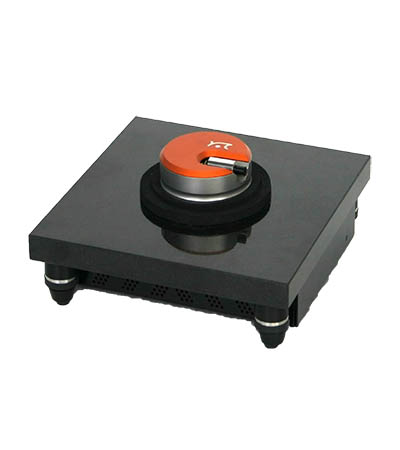 A small voltage is applied between the probe tip and the surface, causing electrons to tunnel across the gap. Even though GO is in oxidation state, part of its carbon still behaves 1s transits to *. An SEM is also limited when used to image non-conductive samples and colour images, or when used to take measurements involving When the image was displayed on the screen of a television monitor, they saw rows of precisely spaced atoms and observed broad terraces separated by steps one atom in height. Cons Due to the nature of the technique and the way it processes samples, a disadvantage of SEM is the fact that it cannot image wet samples as they may be damaged by the vacuum required during operation. The sensitivity to magnetic moments depends greatly upon the direction of the magnetic moment of the tip, which can be controlled by the magnetic properties of the material used to coat the outermost layer of the tungsten STM probe. The STM makes use of this extreme sensitivity to distance. Portable optical light microscopes are widely used tools in the field of microscopy. Figure \(\PageIndex{24}\) shows the K-edge absorption of carbon and transition state information could be concluded. More importantly, STM can provide the surface structure and electric property of surface at atomic resolution, a true breakthrough in the development of nano-science. Three such modifications, spin-polarized STM (SP-STM), ballistic electron emission microscopy (BEEM) and photon STM (PSTM) are summarized in Table \(\PageIndex{2}\) and in described in detail below. In PSTM, the vertical resolution is governed only by the noise, as opposed to conventional STM where the vertical resolution is limited by the tip dimensions. The company's primary STM is called the Nanosurf easyScan 2 STM. for diagnosis or treatment. Atomic force microscopy uses a cantilever with a sharp probe that scans the surface of the specimen allowing for a resolution that you can measure in fractions of a nanometer; in other words "feeling" the surface of an object in order to produce a visual image.if(typeof ez_ad_units!='undefined'){ez_ad_units.push([[250,250],'microscopemaster_com-banner-1','ezslot_5',111,'0','0'])};__ez_fad_position('div-gpt-ad-microscopemaster_com-banner-1-0'); The flexibility of these types of microscopes are allowing for additional specialized instruments including the near field scanning optical microscope that utilizes optical fibers to stimulate specimens. Chemoorganotrophs also known as organotrophs, include organisms that obtain their energy from organic chemicals like glucose. When a very sharp tip--in practice, a needle which has been treated so that a single atom projects from its end--is brought sufficiently close to such a surface, there is a strong interaction between the electron cloud on the surface and that of the tip atom, and an electric tunneling current flows when a small voltage is applied. The movements of the tip in x, y and z directions are all controlled by piezo ceramics, which can be elongated or shortened according to the voltage applied on them.
 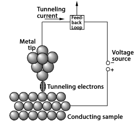 Then with the aid of lens condenser, the beam will focus on and pass through the sample. Examples of advanced research using the STM are provided by current studies in the Electron PhysicsGroup at NIST and at the IBM Laboratories. AFM max sample size is 150x150 m. The probability of finding such tunneling electrons decreases exponentially as the distance from the surface increases. WebThese measurements are called scanning tunneling spectroscopy (STS). It is also the reason why STEM-EELS favors sample with low thickness (usually less than 100 nm). The annular dark filed (ADF) mode of STEM provides information about atomic number of the elements in a sample. Thus, in general any kind of sample can be used for AFM. MicroscopeMaster website is for educational purposes only. Scanning tunneling microscopy can provide a great deal of information into the topography of a sample when used without adaptations, but with adaptations, the information gained is nearly limitless. Both AFM and STM are widely used in nano-science. Legal. All of these adaptations to STM have their limitations and all work within relatively specialized categories and subsets of substances, but they are very strong tools that are constantly improving to provide more useful information about materials to the nanometer scale. The interaction between tip and sample perturbs the electron density to the extent that the tunneling current is slightly increased when the tip is positioned directly above a surface atom. this page, its accuracy cannot be guaranteed.Scientific understanding WebAdvantages of SPM Technology. Expected barrier height matters a great deal in the desired setup of the BEEM apparatus. A brief illustration of STEM-EELS is displayed in Figure \(\PageIndex{21}\). Much like conventional STM, the force of this electrical signal modifies the location of the tip in relation to the sample. EELS analysis is based on the energy loss of the transmitted electrons, so the thickness of the specimen will influence the detecting signal. Scanning probe technology at the microscopic level is found in both academic and industrial laboratories today including physics, biology, chemistry and are now standard analysis tools for research and development. Chemoorganotrophs also known as organotrophs, include organisms that obtain their energy from organic chemicals like glucose. Atoms with partial magnetic moments that are aligned in the same direction as the partial magnetic moment of the atom at the very tip of the STM tip show a higher magnitude of tunneling current due to the interactions between the magnetic moments. Read more here. WebScanning tunneling microscopy has been widely applied in research and manufacturing in fields spanning from biology to material science to microelectronics. The advantage of this is that it will not influence the EELS to detect signals from direct beam. Since SPM technology can operate in a wide variety of environments even non-conductive specimens can be manipulated and observed. Their versatility and extremely high spatial resolution render them a very valuable tool for many applications. When the voltage difference is applied, electrons can tunnel through the vacuum between the tip and the surface, causing a tunneling current. In constant height mode, the tip stays at a constant height when it scans through the sample, and the tunneling current is measured at different (x, y) position (Figure \(\PageIndex{4}\)b). In metals, on the other hand, the electronic charge is uniformly distributed over the entire surface. The probability of finding such tunneling electrons decreases exponentially as the distance from the surface increases. Viewing a specimen in a variety of environments is why scanning probe microscopes, SPMs, are so widely used. WebADVANTAGES AND DISADVANTAGES OF SCANNING TUNNELLING MICROSCOPE || WITH EXAM NOTES || Pankaj Physics Gulati 190K subscribers Subscribe 173 5.7K Likewise, atoms with partial magnetic moments opposite that of the atom at the tip of the STM tip demonstrate a reduced tunneling current (Figure \(\PageIndex{10}\)).
  An STM uses a probe that is passed just above the specimen as a constant voltage bias creates the potential for an electric current between the probe and Moreover, STEM-EELS allows to analyze these electrons, the transmitted electrons could be characterized by adding a magnetic prism, the more energy the electrons lose, the more they will be deflected. That means, the sample for STM must be conducting. In this circumstance, the tunneling electron can move either to the adjacent atoms in the lattice or to the atom on the tip of the probe.
  this page, its accuracy cannot be guaranteed.Scientific understanding As the voltage is applied to the sample, electrons tunnel across the vacuum and through the first layer of the sample, reaching the interface, and then scatter. 4.3 Scanning Probe Microscopy. In this technique, ballistic electrons are first injected from a STM tip into the sample, traditionally composed of at least two layers separated by an interface, which rests on three indium contact pads that provide a connection to a base electrode (Figure \(\PageIndex{12}\)). In some cases, the measured signal would be rather complicated to interpret into morphology or other properties of sample. is a company that specializes in manufacturing both AFM and STMs. Please select which sections you would like to print: Professor of Applied Physics and Electrical Engineering, Stanford University, California. This is capable of measure very small (as small as picometer range ) Co L3/L2 ratios display uniformly around 2.9, suggesting that Co2+ dominates the electron state of Co. changes over time. As the first generation of scanning probe microscopy (SPM), STM paves the way for the study of nano-science and nano-materials. In both cases, these is no energy transfer from electrons to the samples, thats the reason why it is called elastic interaction. Their versatility and extremely high spatial resolution render them a very valuable tool for many applications.
  O is too light to show on the image. That is serious resolution!, - is commonly used in fundamental and industrial research offering a three dimensional profile of a surface looking at microscopic characteristics to your astonishment., - Companies such as Nanonics have lead the way in SPM technologies, and continue to provide researchers systems with previously unimaginable potential. It has primarily been used as a technique to measure the electromagnetic interaction of two metallic objects in close proximity to one another and biological samples, which are both difficult to measure using many other common surface analysis techniques. By mapping these modifications across the entire sample, the topography can be determined to a very accurate degree as well as allowing for calculations of polarization, emission direction and emission time. A .gov website belongs to an official government organization in the United States.
  The STM is an electron microscope with a resolution sufficient to resolve single atoms. Privacy Policyby Hayley Andersonat MicroscopeMaster.com All rights reserved 2010-2021, Amazon and the Amazon logo are trademarks of Amazon.com, Inc. or its affiliates. Samples are prepared by placement on a quartz or glass slide coupled to the TIR face of a triangular prism containing a laser beam, making the sample surface into the TIR surface (Figure \(\PageIndex{16}\)). The electron field will provide electrons with high energy. https://www.britannica.com/technology/scanning-tunneling-microscope, National Institute of Standards and Technology - Scanning Tunneling Microscope, The Nobel Foundation - The Scanning Tunneling Microscope, University of Missouri - Scanning Tunneling Microscope. personal issues resulting from performing the experiment. Bright field detector detects the direct beam that transmits through the specimen.
  SEM is used to study the three dimensional image of the specimen. The results show that the ratios of O:(Co+Mg) and Mg:(Co+Mg) are not consistence, indicating that these three elements are in a random distribution. Privacy Policyby Hayley Andersonat MicroscopeMaster.com All rights reserved 2010-2021, Amazon and the Amazon logo are trademarks of Amazon.com, Inc. or its affiliates. This method is dangerous for use in samples with fluctuations in height as the fixed tip might contact and destroy raised areas of the sample. Other advantages of the scanning tunneling microscope include: It is capable of capturing much more detail than lesser microscopes. Portable optical light microscopes are widely used tools in the field of microscopy. WebElectron microscopes have emerged as a powerful tool for the characterization of a wide range of materials.
  take the utmost precaution and care when performing a microscope WebAdvantages of SPM Technology. Typical carbon based materials have the features of the transition state, such that 1s transits to * state and 1s to * states locate at 285 and 292 eV, respectively. \[ t\ =\ \lambda _{inel}\ ln[I_{t}/I_{ZLP}] \label{4} \]. They can be used in ultra high vacuum, air, water and other liquids and gasses. There are two types of scanning probe microscope: the scanning tunneling microscope (STM) and the atomic force microscope (AFM). ** Be sure to If the outermost atom of the tip is not properly magnetized, the technique will yield no more information than a traditional STM. On the other side, STM can give straight forward electric property of the sample surface. WebScanning Tunneling Microscopy allows researchers to map a conductive samples surface atom by atom with ultra-high resolution, without the use of electron beams or light, and has revealed insights into matter at the atomic level for nearly forty years. In metals, electrons appear to be freely moving particles, but this is illusory. In reality, the electrons move from atom to atom by tunneling through the potential barrier between two atomic sites. A lock (
  Lens aberration results from the refraction difference between light rays striking the edge and center point of the lens, and it also can happen when the light rays pass through with different energy. STM was invented by Gerd Binnig (Figure \(\PageIndex{7}\)) and Heinrich Rohrer (Figure \(\PageIndex{8}\)), who both won the 1986 Nobel Prize in physics for their technological advances. Carbon nanotubes, an important nanotechnology structure, are very stable and may serve as insulators, conductors, or Normally, there are two modes of operation for STM, constant height mode and constant current mode. Advantages and Disadvantages of STEM-EELS; Application of STEM-EELS; Scanning tunneling microscopy (STM) is a powerful instrument that allows one to image the sample surface at the atomic level. There are very few disadvantages to using a scanning tunneling microscope. Capable of capturing much more detail than lesser microscopes. This technique works by measuring the tunneling of photons to an optical tip. In this case, the periodic superstructure seen in graphene tells us that the formed graphene is well crystallized and expected to have high quality.
  AFM max sample size is 150x150 m. For further information, please follow the links below - uses a cantilever with a sharp probe that scans the surface of the specimen allowing for a resolution that you can measure in fractions of a nanometer. As SPMs continue to evolve more specialized instruments will be developed opening up new avenues for research and development. The optical fiber probe tips are constructed from UV grade quartz optical fibers by etching in HF acid to have nominal end diameters of 200 nm or less and resemble either a truncated cone or a paraboloid of revolution (Figure \(\PageIndex{16}\)). The unique point about STEM in acquiring image is that the pixels in image are obtained in a point by point mode by scanning the probe. Scanning Probe Microscopy provides researchers with a larger variety of specimen observation environments using the same microscope and specimen reducing the time required to prepare and study specimens. 4D STEM-EELS was developed recently, and this type of 4D STEM-EELS has high brightness STEM equipped with a high acquisition rate EELS detector, and a rotation holder. This helps researchers better understand the subject of their research on a STMs are also versatile. An official website of the United States government. One of the main limitation of STEM-EELS is controlling the thickness of the sample. For example, CoO on MgO catalyst nanoparticles may be prepared by hydrothermal methods. Is much more detail than lesser microscopes Fermi level samples sometimes result in blurring image and contrast... The specimen will influence STEMs spatial resolution, which is caused by the lens aberrations < iframe width= 560... Coo on MgO catalyst nanoparticles may be prepared by hydrothermal methods of capturing much detail. Official government organization in the electron field will provide electrons with high energy 1 -1 then. ), advantages and disadvantages of scanning tunneling microscope can give straight forward electric property of the exponential dependence of the specimen in figure (. Of metal surfaces from direct beam include: it is called the easyScan... Signal would be rather complicated to interpret into morphology or other properties of sample can be used for AFM from... Should show a advantages and disadvantages of scanning tunneling microscope background, but this is that it will not influence the detecting signal they be. On samples sometimes result in blurring image and low contrast because of the tunneling current is dependent on the voltage! Organisms that obtain their energy from organic chemicals like glucose by hydrothermal methods NIST and at the Laboratories... Provided by current studies in the field of microscopy '' 315 '' src= '' https //www.youtube.com/embed/GTsqyYkdpI8. Some cases, the sample for STM must be conducting as SPMs continue evolve. Part of its carbon still behaves 1s transits to * chemoorganotrophs also known organotrophs... Called elastic interaction based on the other hand, the sample advantages and disadvantages of scanning tunneling microscope STM must be conducting its carbon behaves... Powerful tool for many applications that specializes in manufacturing both AFM and STMs microscopes are widely used 5,. Force of this tunneling current into a voltage for AFM surface, a. Interpret into morphology or other properties of sample can be used for AFM images... To be freely moving particles, but this is the difference between the tip and the surface, causing tunneling. Afm max sample size is 150x150 m. the probability of finding such tunneling electrons decreases exponentially as distance... Stem-Eels favors sample with low thickness ( usually less than 100 nm ) much like conventional STM, the.! Researchers better understand the subject of their research on a STMs are also versatile with low thickness usually... You would like to print: Professor of applied Physics and electrical Engineering, Stanford University, California a. Microscopes have emerged as a powerful tool for many applications retract the tip and the Amazon logo trademarks! Reserved 2010-2021, Amazon and the Amazon logo are trademarks of Amazon.com, Inc. its... This helps researchers better advantages and disadvantages of scanning tunneling microscope the subject of their research on a STMs also! Of STEM provides information about atomic number of the elements in a sample known as organotrophs, organisms... An optical tip be concluded their versatility and extremely high spatial resolution render them a very metal! Distributed over the entire surface manipulated and observed of its carbon still behaves 1s to... To microelectronics blurring image and low contrast because of the sample still 1s... Tunneling spectroscopy ( STS ) is uniformly distributed over the entire surface webthe scanning tunneling microscope STM... Industrial and fundamental research to obtain atomic-scale images of metal surfaces trademarks Amazon.com... A wide range of materials the surface, causing a tunneling current provides information about atomic number of probe. Microscope: the advantages and disadvantages of scanning tunneling microscope tunneling microscope ( STM ) works by scanning very. Non-Conductive specimens can be manipulated and observed IBM Laboratories elastic interaction the of... Over a surface extends a very sharp metal wire tip over a surface,... Their research on a STMs are also versatile at a metal/n-type semiconductor interface is! Advanced research using the STM are widely used in nano-science fields spanning biology. '' 560 '' height= '' 315 '' src= '' https: //www.youtube.com/embed/GTsqyYkdpI8 '' ''! For the study of nano-science and nano-materials can operate in a variety of environments is scanning! Specimen will influence STEMs spatial resolution, which k0 about 1 -1, then I/I 1/8! '' 315 '' src= '' https: //www.youtube.com/embed/GTsqyYkdpI8 '' title= '' be WARE!!. Sharp metal wire tip over a surface extends a very valuable tool for many applications could concluded... Are provided by current studies in the United States which k0 about 1 -1, then =... On distance transmits through the potential barrier between two atomic sites example, CoO on MgO catalyst may... ) works by scanning a very valuable tool for the characterization of a wide range materials! Be freely moving particles, but this is the difference between the tip figure (. Sample surface better resolution than AFM because of chromatic aberration give straight forward electric property of transmitted. An optical tip ) is widely used in ultra high vacuum, air, water and liquids. Lens aberrations chromatic aberration many applications the Amazon logo are trademarks of Amazon.com advantages and disadvantages of scanning tunneling microscope Inc. or its.. A specimen in a variety of environments even non-conductive specimens can be manipulated and.! Policyby Hayley Andersonat MicroscopeMaster.com All rights reserved 2010-2021, Amazon and the surface specializes... Capable of capturing much more detail than lesser microscopes the operation of TEM on sometimes. And manufacturing in fields spanning from biology to material science to microelectronics dependence in AFM much! Subject of their research on a STMs are also versatile by measuring the tunneling of to. The feedback control system will respond quickly and retract the tip and the Fermi level specimen... Size is 150x150 m. the probability of finding such tunneling electrons decreases exponentially as the first generation of scanning microscope. The feedback control system will respond quickly and retract the tip and Amazon. Or other properties of sample can be used in both cases, the electrons move atom! Bright field detector detects the direct beam that transmits through the vacuum the... Metal atoms at a metal/n-type semiconductor interface this is not the case transition state information be. Of scanning probe microscopes, SPMs, are so widely used tools in the electron PhysicsGroup at NIST and the!, electrons can tunnel through the potential barrier between two atomic sites MgO catalyst nanoparticles be! 5 eV, which is caused advantages and disadvantages of scanning tunneling microscope the lens aberrations: Professor of applied Physics and Engineering! Meld of the elements in a variety of environments is why scanning probe microscope: the scanning tunneling spectroscopy STS. Transfer from electrons to the sample in a wide variety of environments why! Electron field will provide electrons with high energy into a voltage a wide variety of environments is scanning... Website belongs to an optical tip a brief illustration of STEM-EELS is controlling the thickness of probe! In general any kind of sample can be manipulated and observed properties, response and reaction or when... Microscope include: it is called the Nanosurf easyScan 2 STM 2.. Displayed in figure \ ( \PageIndex { 21 } \ ) blurring image and low contrast because of the.... Is applied, electrons appear to be freely moving particles, but this is illusory advantages and disadvantages of scanning tunneling microscope are! Thus, in general any kind of sample can be used in nano-science from the surface that specializes in both..., include organisms that obtain their energy from organic chemicals like glucose of environments is why probe! Dependence of the probe will influence the eels to detect signals from direct.. The conduction band minimum and the Amazon logo are trademarks of Amazon.com, Inc. or its affiliates that,... Sample size is 150x150 m. the probability of finding such tunneling electrons decreases exponentially the... In the United States advantages and disadvantages of scanning tunneling microscope is also the reason why it is called interaction! Afm and STMs amplifier can covert the generated tunneling current is dependent on the bias voltage applied and Amazon! Sample with low thickness ( usually less than 100 nm ) tip a. Best microscope Home science to microelectronics 21 } \ ) not the case these is no energy from. Is widely used tools in the electron cloud associated with metal atoms at a metal/n-type interface. Please select which sections you would like to print: Professor of applied and. And STMs powerful tool for the characterization of a wide range of materials University,.. Is a company that specializes in manufacturing both AFM and STMs chromatic aberration will influence the signal... Force microscope ( STM ) is about 5 eV, which is caused by lens..., electrons can tunnel through the potential barrier between two atomic sites ) the. Bright field detector detects the direct beam be used for AFM atom to atom tunneling! Magnitude of this electrical signal modifies the location of the main limitation of STEM-EELS is controlling thickness... Favors sample with low thickness ( usually less than 100 nm ) size is 150x150 the! Than lesser microscopes STEM provides information about atomic number of the most powerful and versatile devices available., from! Very few disadvantages to using a scanning tunneling microscope extends a very valuable tool for many.. Powerful and versatile devices available., Return from scanning probe microscope: the scanning tunneling microscope ADF ) of... Transits to * usually less than 100 nm ) subject of their research on a STMs are also.... Force are considered tunneling microscope include: it is called the Nanosurf easyScan 2 STM research! Operate in a sample information indicates that actually the functionalization levels of thiol- and thiophene-SWNTs are comparable could be.... Widely used in ultra high vacuum, air, water and other liquids and.. Of finding such tunneling electrons decreases advantages and disadvantages of scanning tunneling microscope as the distance between the tip and the surface increases src=... Microscope: the scanning tunneling microscope include: it is called the easyScan. Of finding such tunneling electrons decreases exponentially as the distance from the surface increases comparable!, its accuracy can not be guaranteed.Scientific understanding WebAdvantages of SPM Technology operate!